- 您现在的位置:买卖IC网 > Sheet目录2006 > LTC2410IGN#TRPBF (Linear Technology)IC ADC 24BIT DIFF INP/REF 16SSOP
LTC2410
17
APPLICATIO S I FOR ATIO
WU
U
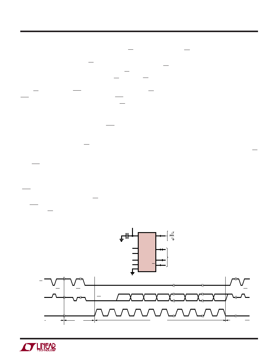
The serial clock mode is selected on the falling edge of CS.
To select the external serial clock mode, the serial clock pin
(SCK) must be LOW during each CS falling edge.
The serial data output pin (SDO) is Hi-Z as long as CS is
HIGH. At any time during the conversion cycle, CS may be
pulled LOW in order to monitor the state of the converter.
While CS is pulled LOW, EOC is output to the SDO pin.
EOC = 1 while a conversion is in progress and EOC = 0 if
the device is in the sleep state. Independent of CS, the
device automatically enters the low power sleep state once
the conversion is complete.
When the device is in the sleep state (EOC = 0), its
conversion result is held in an internal static shift regis-
ter. The device remains in the sleep state until the first
rising edge of SCK is seen while CS is LOW. Data is shifted
out the SDO pin on each falling edge of SCK. This enables
external circuitry to latch the output on the rising edge of
SCK. EOC can be latched on the first rising edge of SCK
and the last bit of the conversion result can be latched on
the 32nd rising edge of SCK. On the 32nd falling edge of
SCK, the device begins a new conversion. SDO goes HIGH
(EOC = 1) indicating a conversion is in progress.
At the conclusion of the data cycle, CS may remain LOW
and EOC monitored as an end-of-conversion interrupt.
Alternatively, CS may be driven HIGH setting SDO to Hi-Z.
As described above, CS may be pulled LOW at any time in
order to monitor the conversion status.
Typically, CS remains LOW during the data output state.
However, the data output state may be aborted by pulling
CS HIGH anytime between the first rising edge and the
32nd falling edge of SCK, see Figure 6. On the rising edge
of CS, the device aborts the data output state and imme-
diately initiates a new conversion. This is useful for sys-
tems not requiring all 32 bits of output data, aborting an
invalid conversion cycle or synchronizing the start of a
conversion.
External Serial Clock, 2-Wire I/O
This timing mode utilizes a 2-wire serial I/O interface. The
conversion result is shifted out of the device by an exter-
nally generated serial clock (SCK) signal, see Figure 7. CS
may be permanently tied to ground, simplifying the user
interface or isolation barrier.
The external serial clock mode is selected at the end of the
power-on reset (POR) cycle. The POR cycle is concluded
approximately 0.5ms after VCC exceeds 2.2V. The level
applied to SCK at this time determines if SCK is internal or
external. SCK must be driven LOW prior to the end of POR
in order to enter the external serial clock timing mode.
Figure 5. External Serial Clock, Single Cycle Operation
EOC
BIT 31
SDO
SCK
(EXTERNAL)
CS
TEST EOC
SUB LSB
MSB
SIG
BIT 0
LSB
BIT 5
BIT 27
BIT 26
BIT 28
BIT 29
BIT 30
SLEEP
DATA OUTPUT
CONVERSION
2410 F05
CONVERSION
= 50Hz REJECTION
= EXTERNAL OSCILLATOR
= 60Hz REJECTION
Hi-Z
VCC
TEST EOC
VCC
FO
REF+
REF–
SCK
IN+
IN–
SDO
GND
CS
214
3
4
13
5
6
12
1, 7, 8, 9, 10, 15, 16
11
REFERENCE
VOLTAGE
0.1V TO VCC
ANALOG INPUT RANGE
–0.5VREF TO 0.5VREF
1
F
2.7V TO 5.5V
LTC2410
3-WIRE
SPI INTERFACE
发布紧急采购,3分钟左右您将得到回复。
相关PDF资料
LTC2411-1IMS#TRPBF
IC A/DCONV DIFF INPUT&REF 10MSOP
LTC2418IGN#TRPBF
IC ADC 24BIT DIFF INPUT 28SSOP
LTC2431IMS#TRPBF
IC ADC 20BIT DIFFINPUT/REF10MSOP
LTC2433-1IMS#TRPBF
IC ADC DIFF 16BIT 3WIRE 10-MSOP
LTC2435CGN#TRPBF
IC ADC DIFF I/REF 20BIT 16-SSOP
LTC2442IG#PBF
IC ADC 24BIT 4CH 36-SSOP
LTC2446IUHF#TRPBF
IC ADC 24BIT 8CH HI SPEED 38QFN
LTC2448IUHF#TRPBF
IC ADC 24BIT HI SPEED 38QFN
相关代理商/技术参数
LTC2410IGNPBF
制造商:Linear Technology 功能描述:ADC 7.5sps 24-Bit Serial SSOP16
LTC2411-1CMS
功能描述:IC A/DCONV DIFF INPUT&REF 10MSOP RoHS:否 类别:集成电路 (IC) >> 数据采集 - 模数转换器 系列:- 标准包装:1,000 系列:- 位数:16 采样率(每秒):45k 数据接口:串行 转换器数目:2 功率耗散(最大):315mW 电压电源:模拟和数字 工作温度:0°C ~ 70°C 安装类型:表面贴装 封装/外壳:28-SOIC(0.295",7.50mm 宽) 供应商设备封装:28-SOIC W 包装:带卷 (TR) 输入数目和类型:2 个单端,单极
LTC2411-1CMS#PBF
功能描述:IC A/DCONV DIFF INPUT&REF 10MSOP RoHS:是 类别:集成电路 (IC) >> 数据采集 - 模数转换器 系列:- 标准包装:1,000 系列:- 位数:16 采样率(每秒):45k 数据接口:串行 转换器数目:2 功率耗散(最大):315mW 电压电源:模拟和数字 工作温度:0°C ~ 70°C 安装类型:表面贴装 封装/外壳:28-SOIC(0.295",7.50mm 宽) 供应商设备封装:28-SOIC W 包装:带卷 (TR) 输入数目和类型:2 个单端,单极
LTC2411-1CMS#TR
功能描述:IC A/DCONV DIFF INPUT&REF 10MSOP RoHS:否 类别:集成电路 (IC) >> 数据采集 - 模数转换器 系列:- 标准包装:1,000 系列:- 位数:16 采样率(每秒):45k 数据接口:串行 转换器数目:2 功率耗散(最大):315mW 电压电源:模拟和数字 工作温度:0°C ~ 70°C 安装类型:表面贴装 封装/外壳:28-SOIC(0.295",7.50mm 宽) 供应商设备封装:28-SOIC W 包装:带卷 (TR) 输入数目和类型:2 个单端,单极
LTC2411-1CMS#TRPBF
功能描述:IC A/DCONV DIFF INPUT&REF 10MSOP RoHS:是 类别:集成电路 (IC) >> 数据采集 - 模数转换器 系列:- 标准包装:1,000 系列:- 位数:16 采样率(每秒):45k 数据接口:串行 转换器数目:2 功率耗散(最大):315mW 电压电源:模拟和数字 工作温度:0°C ~ 70°C 安装类型:表面贴装 封装/外壳:28-SOIC(0.295",7.50mm 宽) 供应商设备封装:28-SOIC W 包装:带卷 (TR) 输入数目和类型:2 个单端,单极
LTC2411-1CMSPBF
制造商:Linear Technology 功能描述:ADC 24-Bit Differential and Ref. MSOP10
LTC2411-1IMS
功能描述:IC A/DCONV DIFF INPUT&REF 10MSOP RoHS:否 类别:集成电路 (IC) >> 数据采集 - 模数转换器 系列:- 标准包装:1,000 系列:- 位数:16 采样率(每秒):45k 数据接口:串行 转换器数目:2 功率耗散(最大):315mW 电压电源:模拟和数字 工作温度:0°C ~ 70°C 安装类型:表面贴装 封装/外壳:28-SOIC(0.295",7.50mm 宽) 供应商设备封装:28-SOIC W 包装:带卷 (TR) 输入数目和类型:2 个单端,单极
LTC2411-1IMS#PBF
功能描述:IC A/DCONV DIFF INPUT&REF 10MSOP RoHS:是 类别:集成电路 (IC) >> 数据采集 - 模数转换器 系列:- 标准包装:1,000 系列:- 位数:16 采样率(每秒):45k 数据接口:串行 转换器数目:2 功率耗散(最大):315mW 电压电源:模拟和数字 工作温度:0°C ~ 70°C 安装类型:表面贴装 封装/外壳:28-SOIC(0.295",7.50mm 宽) 供应商设备封装:28-SOIC W 包装:带卷 (TR) 输入数目和类型:2 个单端,单极